Documentation how to generate Gerber files from KiCad for PCB manufacturing at dirtypcbs.
On this link, you can find all information about dirtypcbs info PCB manufacturing.
There are several things need to be done before sending files to manufacture PCBs. Files are generated with KiCad EDA tool, and these are the steps to send your files to dirtypcbs and get your boards as you want.
When board file is finished:
-
Set the origin: Go to Place -> Drill and Place offset and then set the origin near the corner of the board.
-
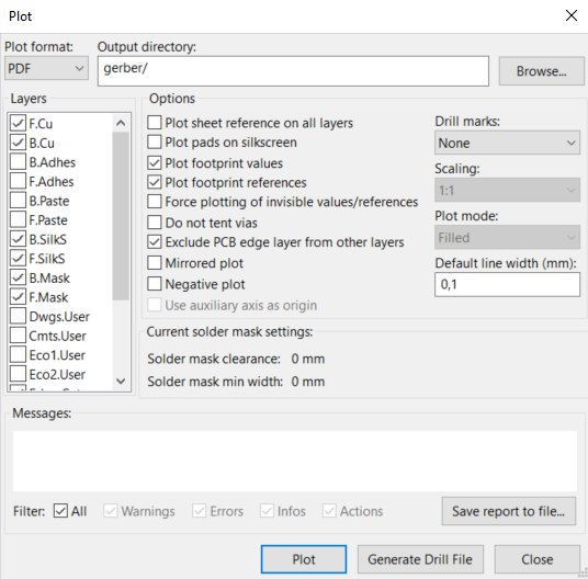
Generate Gerber files PDF: Go to File -> Plot. New Window will appear, like in picture 1. Click on Plot and it will generate Gerber files in PDF form so they could be checked.
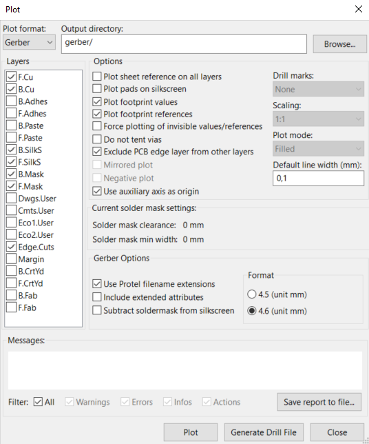
- Generate Gerber files: In the same window click change the Plot format from PDF to Gerber, a window will change and it will look like in picture 2. Some additional boxes need to be checked and everything should be like in picture 2. Then click on Plot and Gerber files will be generated.
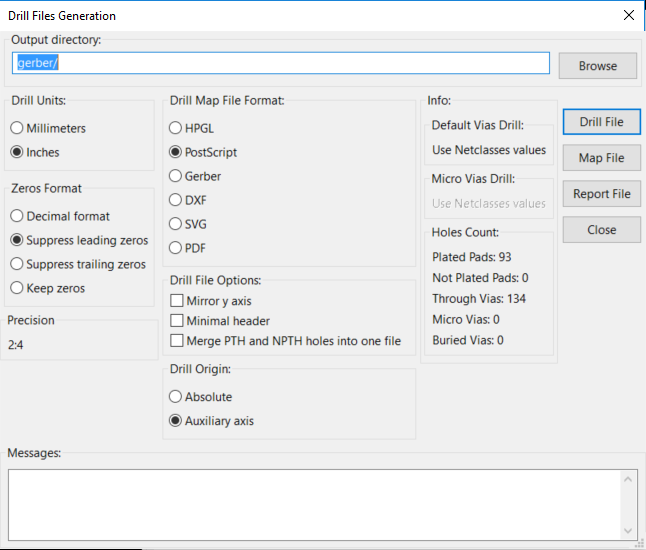
- Generate Drill File: Next click on the Generate Drill File and the new window will appear, like in picture 3. Again everything should be like in picture 3. When everything is set click on Drill File, and Drill file will be generated.
Note: If there are plated and non plated holes in the design please check the "Merge PTH and NPTH holes into one file"
- Change extensions: Extensions of files that contains Edge of the board and Drills needs to be changed. Go to project folder, than go to folder /Gerber and change extensions for Drill file from .drl to .txt and Edge (keepout) file from .gm1 to .gko.
After that everything is ready, just check your Gerber files in Gerber viewer and send them to manufacturing.


